RF 001 - Eigenmode ports and S-parameters
Model definition
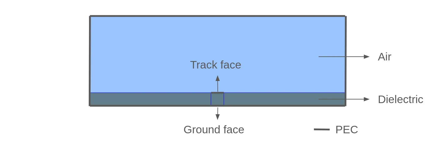
A 3D microstrip track aligned with the x-axis is considered. The corresponding 2D cross-section is illustrated below.
| Component | XYZ dimensions [mm] | Center Z elevation [mm] |
|---|---|---|
| Air box | 10 x 10 x 3 | 0.5/2 + 3/2 |
| Track box | 10 x 0.5 x 0.5 | 0 |
| Dielectric box | 10 x 10 x 0.5 | 0 |
The relative electric permittivity of the dielectric is set to 10 and the working frequency ranges from 5 GHz to 15 GHz.
Use the built-in CAD tools to draw the three boxes in the microstrip stack. The
track is modeled as a perfect conductor and its thickness is neglected. A box is
drawn below the track to create a CAD surface for the track at the dielectric-air
interface.
An alternative setup of the geometry is to provide your .step or .gds file.
Klayout is a popular free tool in the semiconductor industry to easily create
a .gds file for the above geometry.
Simulation setup guide
Step 1 - Create the geometry
In the geometry editor, draw three boxes as detailed above to ready the microstrip geometry.
Step 2 - Define regions, materials and shared expressions
Proceed to the properties editor to define the dielectric and air materials.
Pick the Air material from the materials database and assign it to the corresponding CAD volume.
Create a new material for the dielectric layer and add its permittivity and permeability properties respectively to
and . The track material is not required here as it is modeled
as a perfect conducting face.
For later use, also define a shared expression for the frequency. Name it freq and set it to a default 10e9 Hz. This expression can then be used throughout Allsolve, where applicable.
Step 3 - Define the physics and apply boundary conditions
Proceed to the physics editor and add the electromagnetic waves physics.
In this physics, add interaction perfect conductor and assign it to the surfaces marked as PEC above.
The eigenmode port interaction is now set up at both x-end faces.
Adding an eigenmode port interaction at a port has the following three effects:
- calculate the propagating modes patterns and their propagation constants
- drive the selected mode into the waveguide
- absorb all the power of the selected mode that is reflected back to the port
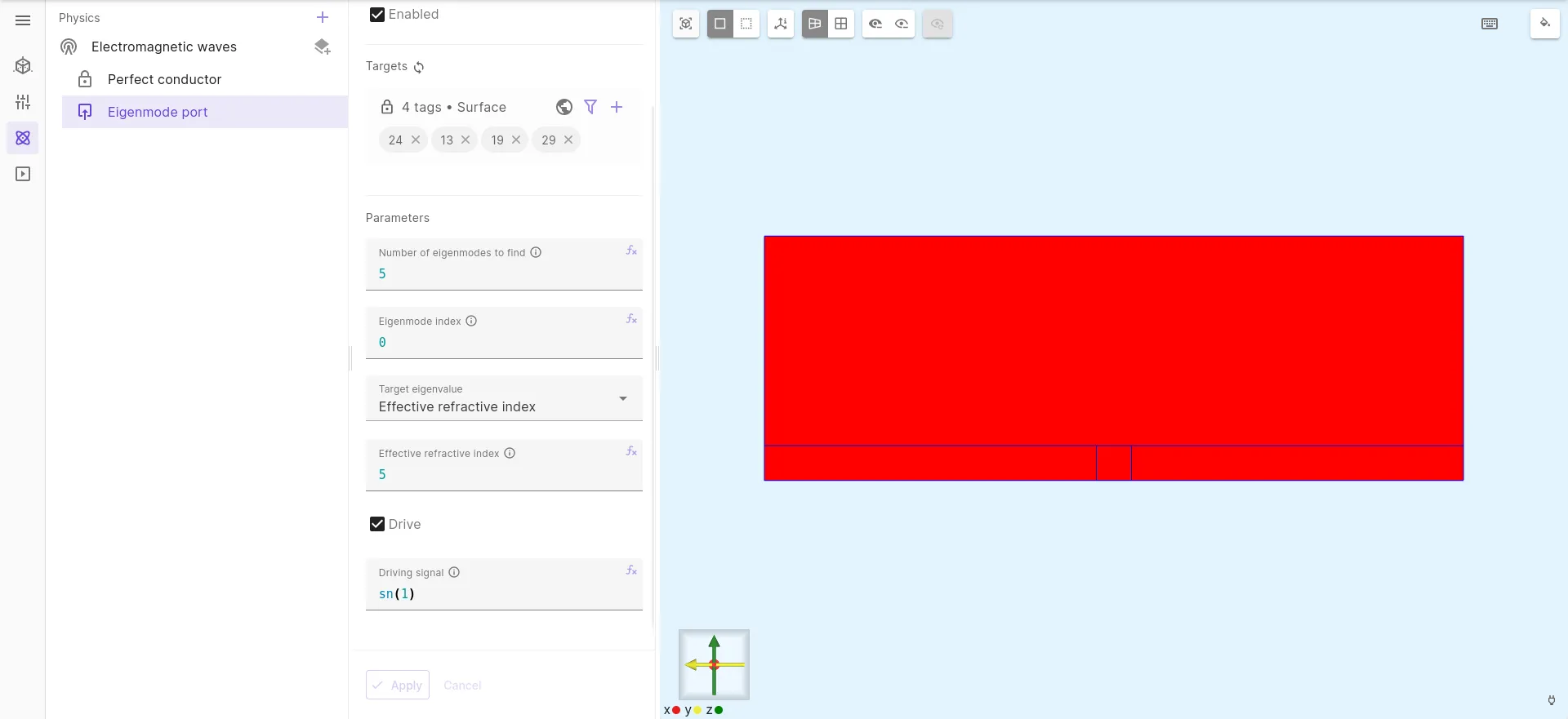
Two eigenmode port interactions should be setup as detailed in the above picture: one interaction per port face.
This type of port performs an eigenmode analysis to find the propagating modes and it can be tuned with the following options:
- the number of eigenmodes to find in the analysis phase can be specified (in this case it is left to the default since only one mode can propagate at the GHz frequencies of interest)
- the eigenmode index allows to choose which mode must be considered at the port out of all modes that have been found by the eigenmode solver. If several modes can propagate, then it is recommended to first run a port mode analysis at simulation time (see below) and come back to this section to select the index of the desired mode. In this case index 0 is selected as it is the first and only propagating mode
- the target eigenvalue can be selected to focus the eigenmode analysis around a propagation constant of interest. This can also be advantageously used to order the eigenmodes, starting from the eigenvalues closest to the target. For convenience one might select the
effective refractive indextarget method: the number that must be provided there is between the relative permittivity of the air and the dielectric medium and is therefore easier to guess correctly without hand calculations - the
drivetick box determines which port is actively powered and which port is only listening and not powered. This option only affects the output electric field profile. It does not affect the S-parameter calculation as the powering for this analysis is determined by Allsolve by powering each port individually one after the other - the product of the
driving signaland the selected magnetic field mode is what is fed into the waveguide. The driving signal can be used to set the port reference phase such as needed for example to drive phased-array antennas. The argument expression can be provided explicitly such as or using shared expressions such as . A shortcutsn(1)orcn(1)can be used respectively as an alias for and where the frequency will be provided at simulation time for a harmonic analysis type. The input power for a phase shifted sine or cosine wave of peak amplitude 1 is 1W time-averaged
Step 4 - Set up the simulation run
Proceed to the Simulations editor and add a new simulation. Add a new mesh that suits your requirements of accuracy.
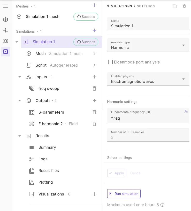
Set up the simulation as detailed in the picture above. The analysis type is harmonic, so that the steady-state solution at a given frequency is obtained.
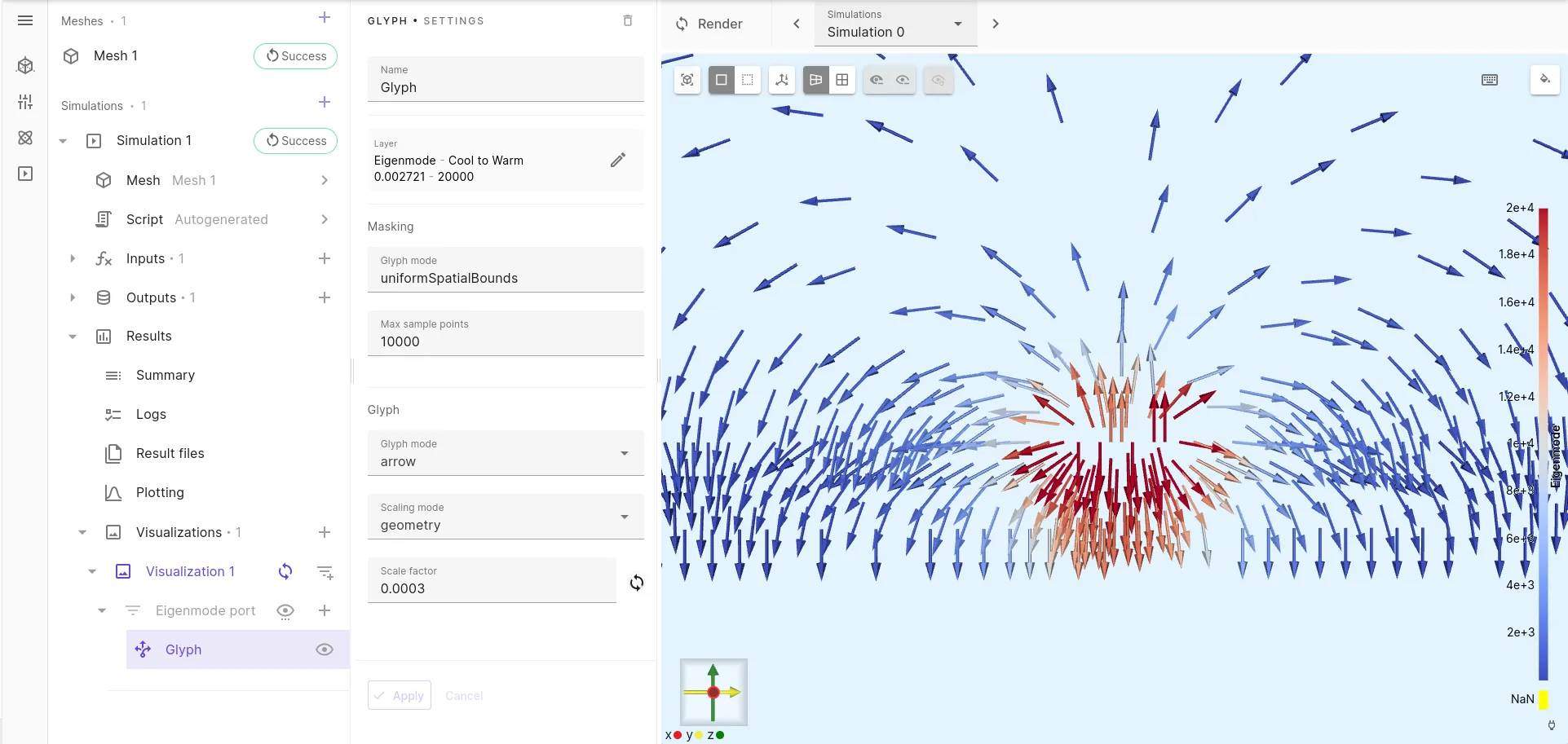
For multimode waveguides, tick the eigenmode port analysis box, then run the simulation and visualize each propagating mode pattern using the glyph filter as illustrated below, or check the log output to get more info regarding the modes found such as the propagation constant and the effective refractive index. Once the desired mode index has been identified, go back to the eigenmode port interaction setup to select the corresponding index (use 0 for the first mode in the list). Don’t forget to untick the eigenmode port analysis before the next run.
In this case, a GHz range driving frequency is used and only a single QTEM mode can propagate, hence the above mode analysis step is not required.
Select as output at least the S-parameters. If you want to visualize the profile of the real part/imaginary part (that is, the harmonic 2/3) of the electric field solution, also add the E field output on the region of interest.
To perform a frequency sweep from 5 GHz to 15 GHz by steps of 1 GHz, add the sweep input linspace(5e9, 15e9, 11).
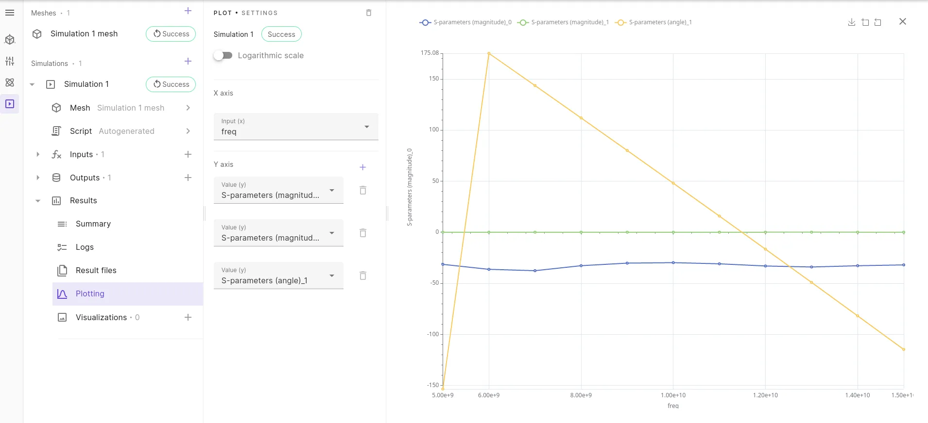
Run the simulation, then go to the plotting option and select for example the S12 angle output to show the microstrip line delay sweep versus frequency illustrated on the picture below. If the simulation is set up properly you should obtain a very low S11 magnitude (in dB) and a close to 0 dB S12 magnitude. The values will get closer to the exact S11 and S12 values as the mesh is refined.