RF 002 - Lumped ports and RLC components
Model definition
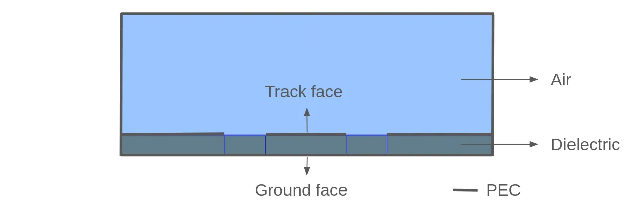
A thin slice of a 3D grounded coplanar waveguide (GCPW) aligned with the x-axis is considered. The corresponding 2D cross-section is illustrated below.
| Component | XYZ dimensions [mm] | Center Z elevation [mm] |
|---|---|---|
| Air box | 0.5 x 10 x 3 | 0.5/2 + 3/2 |
| Track box | 0.5 x 2 x 0.5 | 0 |
| Spacer box | 0.5 x 4 x 0.5 | 0 |
| Dielectric box | 0.5 x 10 x 0.5 | 0 |
The relative electric permittivity of the dielectric is set to 5 and the drive frequency is 10 GHz.
Use the built-in CAD tools to draw the four boxes in the GCPW stack. The
track and ground is modeled as a perfect conductor and its thickness is neglected. A box is
drawn below the track to create a CAD surface for the track at the dielectric-air
interface. Another box is drawn under the track and the spacer to create CAD surfaces
for the grounds on the sides of the track.
An alternative setup of the geometry is to provide your .step or .gds file.
Klayout is a popular free tool in the semiconductor industry to easily create
a .gds file for the above geometry.
Simulation setup guide
Step 1 - Create the geometry
In the geometry editor, draw four boxes as detailed above to ready the GCPW geometry.
Step 2 - Define regions, materials and shared expressions
Proceed to the properties editor to define the dielectric and air materials.
Pick the Air material from the materials database and assign it to the corresponding CAD volume.
Create a new material for the dielectric layer and add its permittivity and permeability properties respectively to
and . The track and ground materials are not required here as they are modeled
as perfect conducting faces.
For later use, also define a shared expression for the waveguide termination resistor. Name it R and set it to a default 50 Ohms. This expression can then be used throughout Allsolve, where applicable.
Step 3 - Define the physics and apply boundary conditions
Proceed to the physics editor and add the electromagnetic waves physics.
In this physics, add interaction perfect conductor and assign it to the surfaces marked as PEC above.
The eigenmode port interaction is now set up at the minimum x-end face. Since only a single mode can propagate at the frequency of interest, most default settings can be left as they are.
Toggle the target eigenvalue to provide the effective refractive index value 5. The actual value for the QTEM that propagates is between the relative permittivity of the air and of the dielectric.
Should an analysis frequency high enough be selected so that another type of mode can propagate, then the one with an effective refractive index closest to 5 will be returned first and selected if the default eigenmode index of 0 is used.
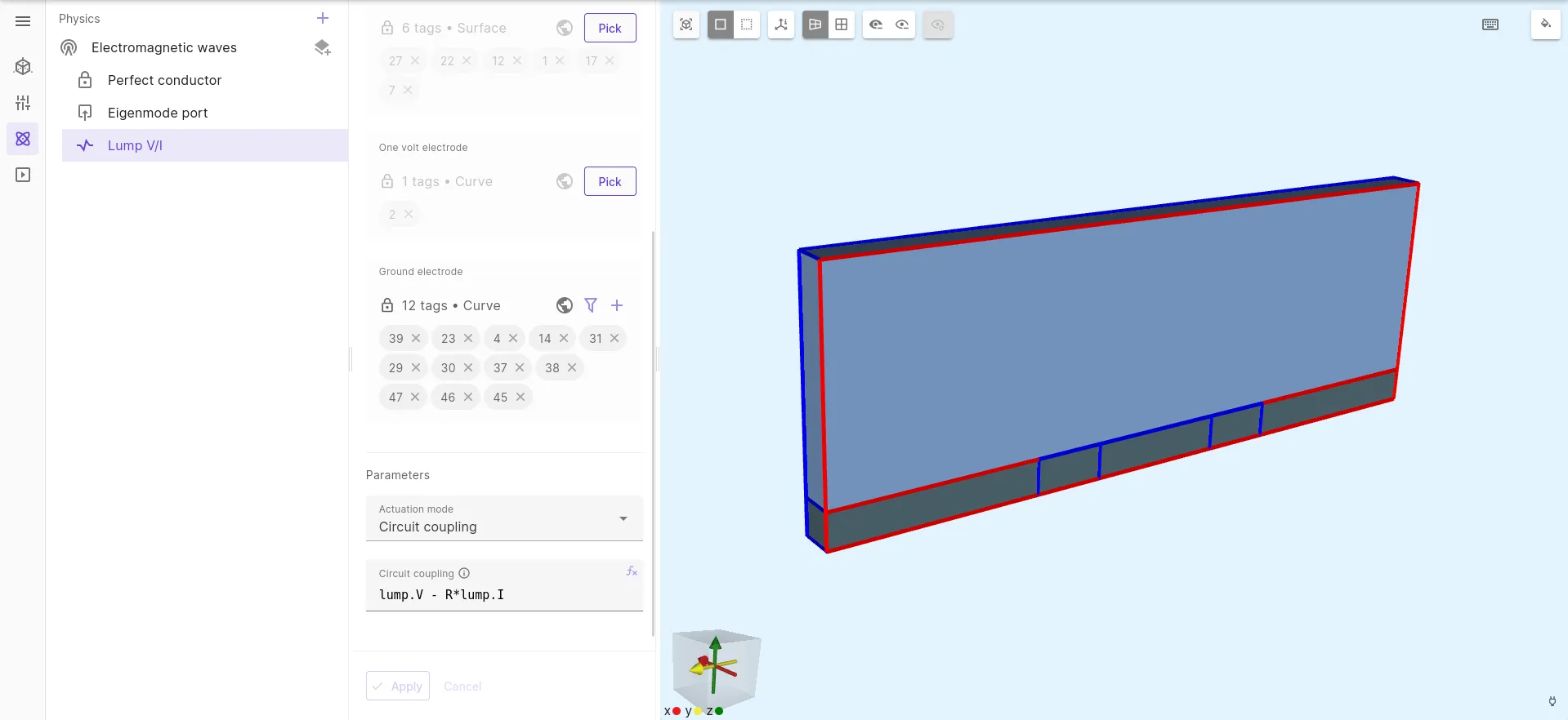
The other end face of the GCPW will in this example not be terminated with an eigenmode port. Instead the lumped port will be explored.
A lumped port works by forcing the tangential electric field at the port face to a profile provided by the user through an electrostatic resolution (user provided 1V and 0V regions are considered and the DC electric field profile between these two regions is computed). The voltage V at the 1V region is readily usable at a lumped port.
The total current I is also readily usable at a lumped port without requiring any user input: it is equal to the current entering the waveguide at the 0V region, or minus the current entering the waveguide at the 1V region. In other words, if one considers the port face as being a current sheet, the current I is positive when it follows the port electric field direction.
The quantities V and I available at the port can be used to connect an RLC circuit at the lumped port or between two lumped ports. In this example, a lumped resistor is connected to the port using equation . Alternatively, connecting an RL and RLC circuit can be done respectively with equation and .
The lumped port setup is illustrated below.
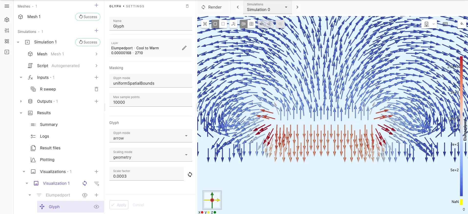
The mode profile at the lumped port for this GCPW is illustrated below.
Step 4 - Set up the simulation run
Proceed to the Simulations editor and add a new simulation. Add a new mesh that suits your requirements of accuracy. Refining the mesh close to the track electrode and the spacer is beneficial for increased accuracy. This can be achieved by refining the track and spacer surfaces or the volumes below. Alternatively a structured mesh can be set up for these volumes to control the exact shape and density of the mesh.
Set up the simulation. The analysis type is harmonic, so that the steady-state solution at a given frequency is obtained.
For multimode waveguides, tick the eigenmode port analysis box, then run the simulation and visualize each propagating mode pattern using the glyph filter similarly as shown above for the lumped port mode, or check the log output to get more info regarding the modes found such as the propagation constant and the effective refractive index. Once the desired mode index has been identified, go back to the eigenmode port interaction setup to select the corresponding index (use 0 for the first mode in the list). Don’t forget to untick the eigenmode port analysis before the next run.
In this case, a 10 GHz driving frequency is used and only a single QTEM mode can propagate, hence the above mode analysis step is not required.
Select as output at least the S-parameters. If you want to visualize the profile of the real part/imaginary part (that is, the harmonic 2/3) of the electric field solution, also add the E field output on the region of interest.
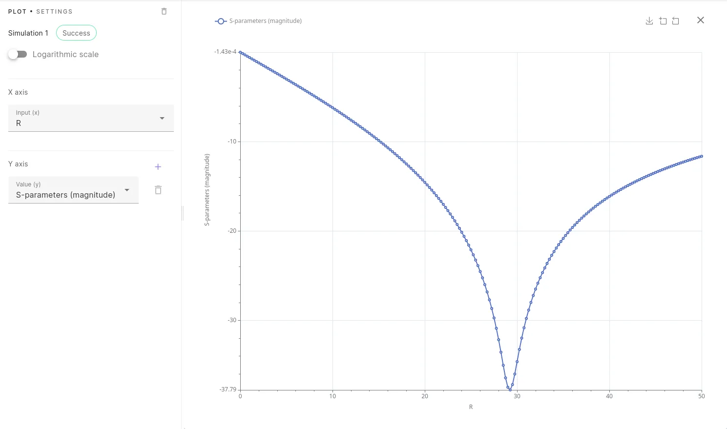
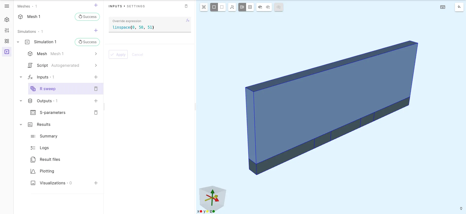
To perform a resistance load sweep from 0 Ohm to 50 Ohm by steps of 1 Ohm, add the sweep input linspace(0, 50, 51) as shown in the picture below. Depending on your plan, the simulations in the sweep will start by more or less large batches at the same time, running on separate hardware instances.
Run the simulation, then go to the plotting option and select the S11 magnitude in dB to show the amount of reflection created by the lumped port R load for various values of R.
The swept curve is shown below: it indicates that terminating the waveguide with a 29.25 Ohm resistor gives load matching with a very low -38 dB mode reflection coming back to the eigenmode port. This is as low as one would get with an eigenmode port used instead of the lumped port and it highlights the accuracy of the lumped port.
The value found matches the GCPW impedance value 29.13 Ohm obtained from usual online calculators.