Patch antenna - RF 003
Prerequisites: complete RF 001 — Eigenmode ports and S-parameters first — it introduces eigenmode ports, S-parameters, and the harmonic sweep workflow used here.
RF patch antennas are widely used in various modern wireless communication systems, from smartphones and laptops to satellites and radar systems. Their compact size, lightweight design, and ease of integration make them a popular choice for engineers. However, designing an efficient and reliable RF patch antenna requires careful consideration of various factors such as operating frequency, bandwidth, gain, and radiation pattern.
Simulation plays a crucial role in the design process, allowing engineers to virtually prototype and optimize antenna performance before physical fabrication. This example demonstrates how Quanscient Allsolve can be used to simulate an RF patch antenna, covering the entire workflow from modeling and simulation setup to running the simulation and analyzing the results. By following this example, you will gain valuable insights into the simulation of RF patch antennas and learn how to leverage Quanscient Allsolve’s capabilities to design and optimize your own antenna systems. This knowledge will enable you to tackle real-world antenna design challenges and develop innovative solutions for various wireless communication applications.
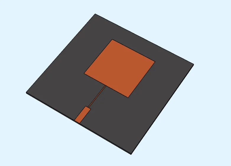
Simulation setup guide
Section titled “Simulation setup guide”Here you’ll find a simplified, example case level guide for setting up a patch antenna simulation in Quanscient Allsolve.
Step 1 - Define variables
Section titled “Step 1 - Define variables”Start out in the Common sidebar by defining the following variables:
| Name | Description | Expression |
|---|---|---|
| Ls | Substrate length [m] | 95.12e-3 |
| hs | Substrate height [m] | 1.57e-3 |
| L50 | 50 ohm transmission line length [m] | 15e-3 |
| W50 | 50 ohm transmission line width [m] | 4.84e-3 |
| ht | Track height [m] | 1e-4 |
| Lqw | Quarter wavelength transformer line length [m] | 24.05e-3 |
| Wqw | Quarter wavelength transformer line length width [m] | 0.72e-3 |
| L | Patch length [m] | 41.08e-3 |
| W | Patch width [m] | L |
| epsilonR | Substrate dielectric constant (relative permittivity) | 2.2 |
| freq | Frequency [Hz] | 2.35e9 |
Step 2 - Build the geometry
Section titled “Step 2 - Build the geometry”- In the
Geometrysection, start building the model by adding Box elements:
| Name | Element type | Center point [m] | Size [m] | Rotation [deg] |
|---|---|---|---|---|
| substrate | Box | X: 0 |
X: Ls |
X: 0 |
Y: 0 |
Y: Ls |
Y: 0 |
||
Z: -hs/2 |
Z: hs |
Z: 0 |
| Name | Element type | Center point [m] | Size [m] | Rotation [deg] |
|---|---|---|---|---|
| 50ohm | Box | X: -Ls/2+L50/2 |
X: L50 |
X: 0 |
Y: 0 |
Y: W50 |
Y: 0 |
||
Z: ht/2 |
Z: ht |
Z: 0 |
| Name | Element type | Center point [m] | Size [m] | Rotation [deg] |
|---|---|---|---|---|
| qw | Box | X: -Ls/2+L50+Lqw/2 |
X: Lqw |
X: 0 |
Y: 0 |
Y: Wqw |
Y: 0 |
||
Z: ht/2 |
Z: ht |
Z: 0 |
| Name | Element type | Center point [m] | Size [m] | Rotation [deg] |
|---|---|---|---|---|
| patch | Box | X: -Ls/2+L50+Lqw+L/2 |
X: L |
X: 0 |
Y: 0 |
Y: W |
Y: 0 |
||
Z: ht/2 |
Z: ht |
Z: 0 |
- Use the Surface rectangle operation to define a port on the substrate boundary in the negative X-plane. First, pick points for the local coordinate axes as shown below:
| Name | Element type | Main axis (green) | Secondary axis (purple) |
|---|---|---|---|
| port surface | Surface rectangle | Origin: left bottom corner point | Point: right bottom corner point |
| End point: left top corner point |
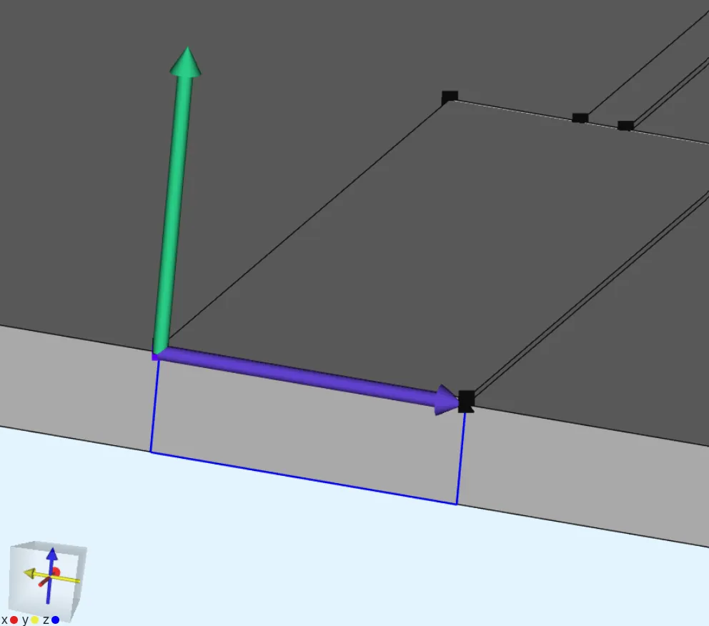
To make a rectangle like above, use these values for offset and size:
| Offset | Size |
|---|---|
Main: 0 |
Main: W50 |
Secondary: -hs |
Secondary: hs |
- Finally, add an airbox around the geometry:
| Name | Element type | Center point [m] | Size [m] | Rotation [deg] |
|---|---|---|---|---|
| airbox | Box | X: 0 |
X: 0.2 |
X: 0 |
Y: 0 |
Y: 0.2 |
Y: 0 |
||
Z: 0.03 |
Z: 0.1 |
Z: 0 |
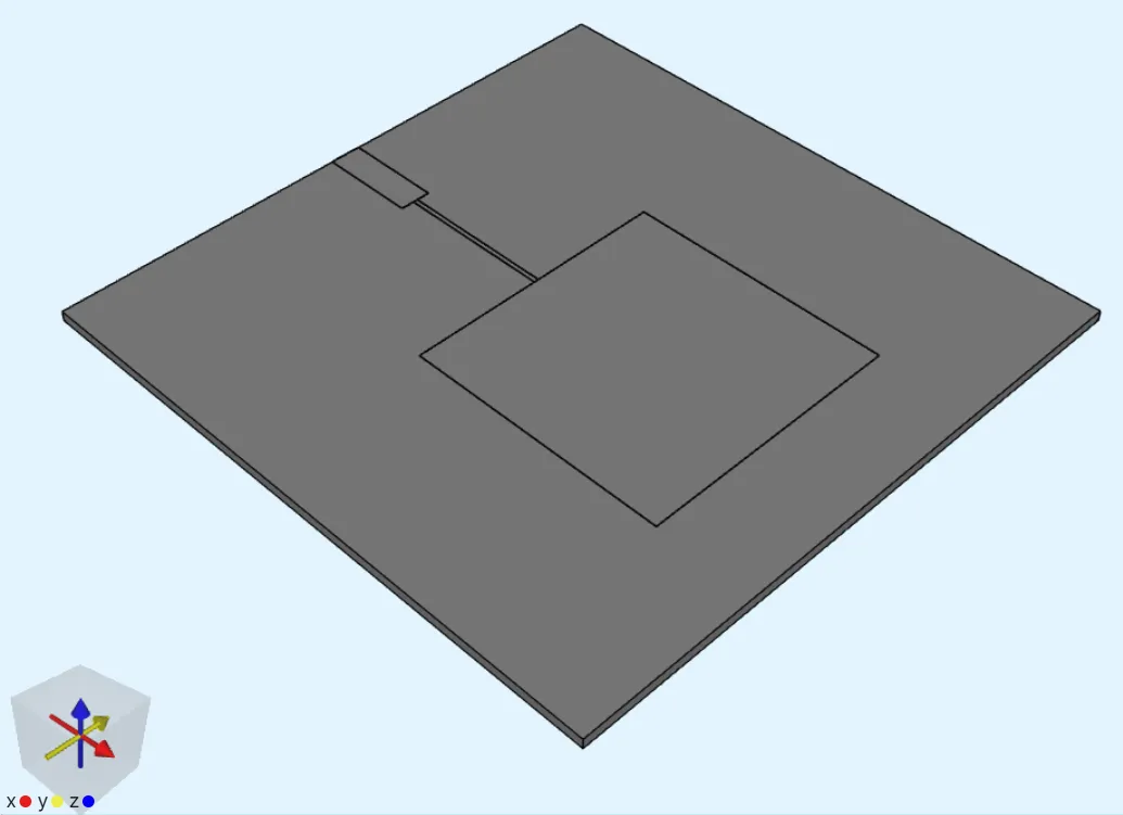
Finished geometry:
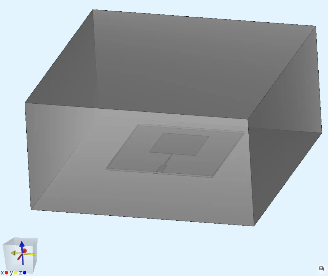
Step 3 - Define the materials
Section titled “Step 3 - Define the materials”After confirming model changes, go to the Physics section to define model materials.
- Assign
Airto the airbox volume. - Assign
Copperto the antenna track volumes (transmission line, quarter wavelength line, and antenna patch). - Assign
FR-4 Dielectricto the substrate volume. - Set the Electric permittivity of FR4 to
epsilonR*epsilon0.
Finished materials:
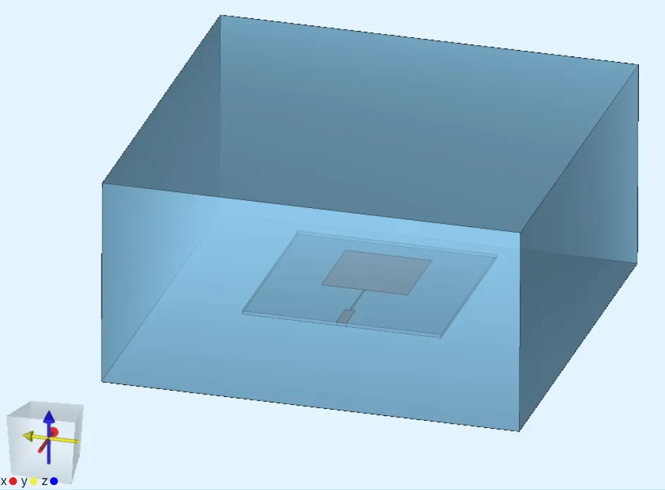
Step 4 - Define the physics
Section titled “Step 4 - Define the physics”Go to the Physics section.
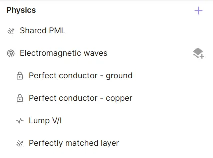
Only the Electromagnetic waves physics is required for this simulation.
-
Add the
Electromagnetic wavesphysics. Let EM waves target default to the whole geometry. -
Add a perfect conductor interaction on the substrate plate bottom surface. This is done to ground the surface.
-
Add a perfect conductor interaction on the antenna track volumes (transmission line, quarter wavelength line, and antenna patch). This is done to prevent simulating electric losses, which are anyway minimal due to high conductivity of copper. If electric losses in the volumes are not interesting, the perfect conductor interaction can be used like this to reduce computational load.
-
Add a Lump V/I interaction for the port:
Interaction Port target One volt electrode Ground electrode Lump V/IPort rectangle surface Top edge curve of port touching track Bottom edge curve of port, touching ground surface Set lump Voltage to
sn(1).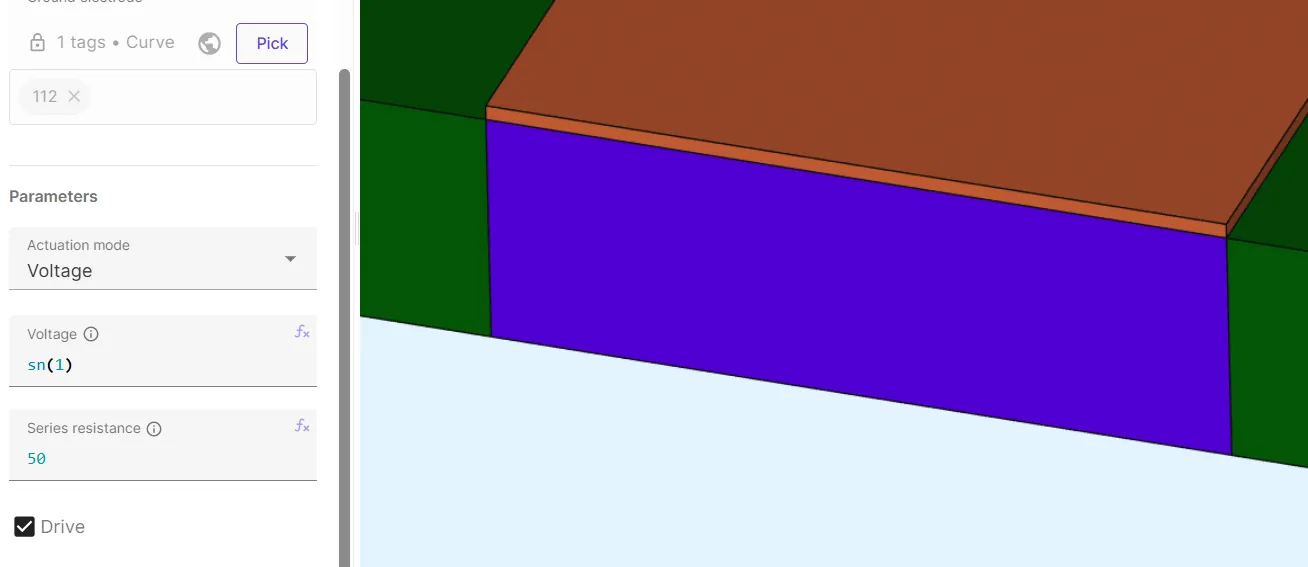
-
Add a Perfectly matched layer interaction on the airbox boundary. Set PML Type to
Box PMLand select all 6 boundary surfaces of the airbox.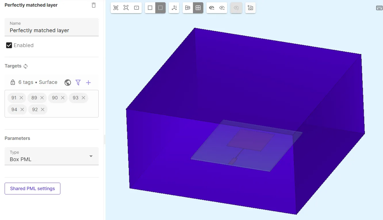
Finished physics tree:
Step 5 - Generate the mesh
Section titled “Step 5 - Generate the mesh”- Go to the Simulations section.
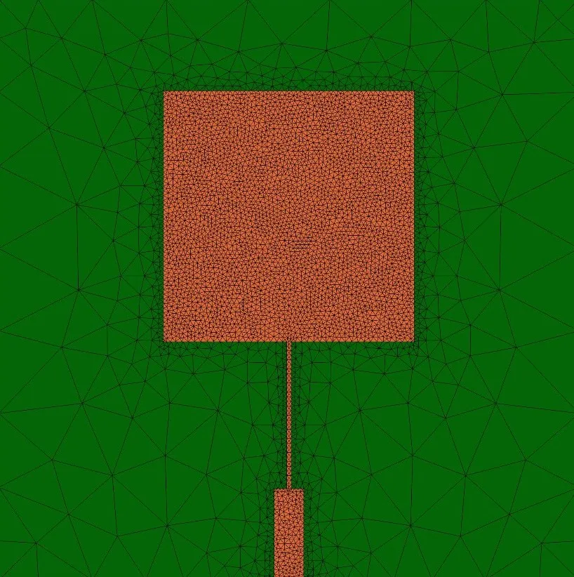
- Create a new mesh.
- Open the collapsible menu for
Mesh element size. - Set Scale factor to
2.
Hide the air box, and check the preview:
Step 6 - Simulate
Section titled “Step 6 - Simulate”In the Simulations section, add a simulation:
- In Simulation settings:
- Set Analysis type to
Harmonic. - Set Fundamental frequency to
freq. - Set Node type to
2 CPU, 32 GB. This ensures the solver has enough memory available to run the simulation.
- Set Analysis type to
- As Mesh, select the mesh you created.
- Inputs:
- Add freq sweep with expression
linspace(2.0e9, 5.0e9, 51)
- Add freq sweep with expression
- Outputs:
- Add
S-parameters - Add
Radiation pattern - Add
E harmonic 2- Select the substrate volume as target.
- Toggle on
Skin only
- Add
Your simulation is now ready to run.
Step 7 - Results
Section titled “Step 7 - Results”In the Simulations section, you can add visualizations to see field output results (Radiation pattern, E field) and plots to see value output results (S-parameters):
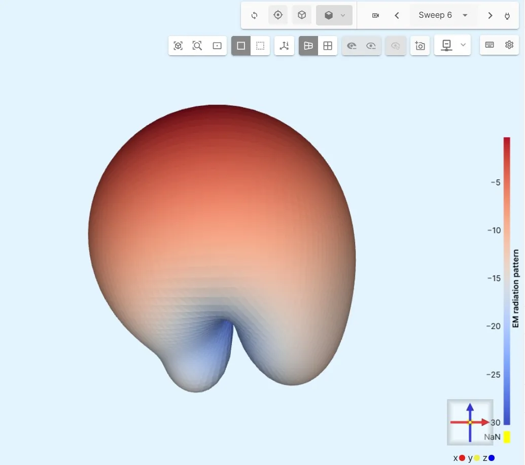
- Radiation pattern at
2.36 GHz:
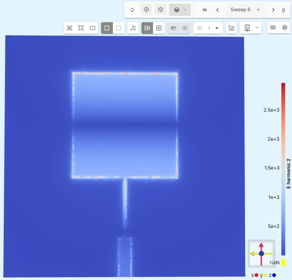
- E field harmonic 2 at
2.36 GHz:
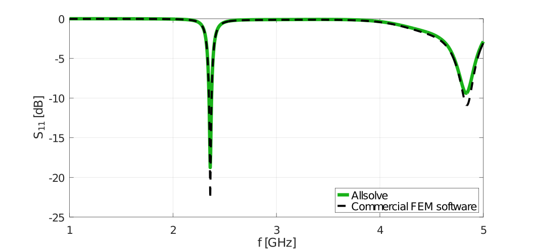
- S-parameter plot made with external software: